12V PWM Controller with Hot-Swap
______________________________________________________________________________________ 17
n-Channel MOSFET Selection
Select the external n-channel MOSFET according to the
applications current level. The MOSFETs on-resis-
tance (R
DS(ON)
) should be chosen low enough to have
a minimum voltage drop at full load to limit the MOSFET
power dissipation. High R
DS(ON)
can cause output rip-
ple if the board has pulsing loads. Determine the
device power-rating requirement to accommodate a
short circuit on the board at startup.
In normal operation, the product of pass MOSFET
R
DS(ON)
and I
IN
should not exceed the circuit-breaker
threshold (600mV).
PWM Controller Design
Procedures
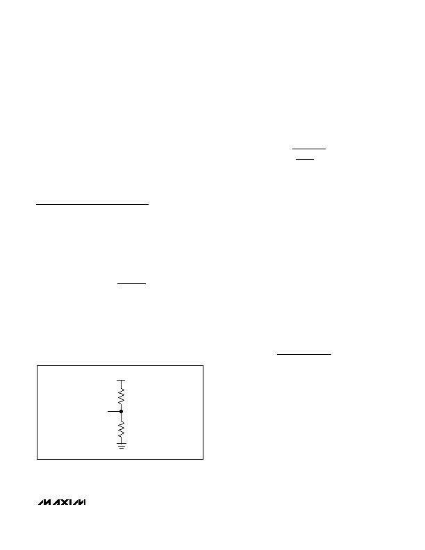
Setting the Undervoltage Lockout
Connect an external resistive divider from PWM_IN to
PUVLO to AGND to override the internal PWM UVLO
divider. The rising threshold at PUVLO is set to 1.220V
with 120mV hysteresis. First, select the PUVLO to
AGND resistor (R2), then calculate the resistor from
PWM_IN to PUVLO (R1), using the following equation:
where V
PWM_IN
is the input voltage at which the con-
verter needs to turn on, V
PUVLO
= 1.220V, and R2 is
chosen to be less than 20k& (see Figure 4).
Leave PUVLO unconnected for the default PWM UVLO
threshold. In this case, an internal voltage-divider moni-
tors the supply voltage at PWM_IN and allows startup
when PWM_IN rises above 7V (typ).
Setting the Output Voltage
Connect a resistive divider from OUT to FB to AGND to
set the output voltage. First, calculate the resistor from
OUT to FB using the guidelines in the Compensation
Design Guidelines section. Once R3 is known, calcu-
late R4 using the following equation:
where V
FB
= 0.8V.
Inductor Selection
Three key inductor parameters must be specified for
operation with the MAX5950: inductance value (L), peak
inductor current (I
PEAK
), and inductor saturation current
(I
SAT
). The minimum required inductance is a function of
operating frequency, input-to-output voltage differential,
and the peak-to-peak inductor current (I
P-P
). Higher
I
P-P
allows for a lower inductor value. A lower induc-
tance value minimizes size and cost and improves
large-signal and transient response, but reduces effi-
ciency due to higher peak currents and higher peak-to-
peak output voltage ripple for the same output
capacitor. A higher inductance increases efficiency by
reducing the ripple current; however, resistive losses
due to extra wire turns can exceed the benefit gained
from lower ripple current levels, especially when the
inductance is increased without also allowing for larger
inductor dimensions. A good rule of thumb is to choose
I
P-P
equal to 30% of the full-load current. Calculate the
inductor using the following equation:
V
IN
and V
OUT
are typical values so that efficiency is
optimum for typical conditions. The switching frequen-
cy is programmable between 100kHz and 1000kHz
(see the Oscillator/Synchronization Input (SYNCIN)/
Synchronization Output (SYNCOUT) section). The
peak-to-peak inductor current, which reflects the peak-
to-peak output ripple, is worst at the maximum input
voltage. See the Output Capacitor Selection section to
verify that the worst-case output current ripple is
acceptable. The inductor saturation current (I
SAT
) is
also important to avoid runaway current during continu-
ous output short-circuit conditions. Select an inductor
with an I
SAT
specification higher than the maximum
peak current.
L
V
V V
V f
I
OUT IN
OUT
IN SW
P P
=
(
)
?/DIV>
?/DIV>
R
R
V
V
OUT
FB
4
3
1
=
?/DIV>
?/DIV>
?/DIV>
?/DIV>
?/DIV>
?/DIV>
R
R
V
V
PWM IN
PUVLO
1
2
1
_
=
?/DIV>
?/DIV>
?/DIV>
?/DIV>
?/DIV>
?/DIV>
?/DIV>
PWM_IN
R1
R2
PUVLO
Figure 4. External PWM UVLO Divider
发布紧急采购,3分钟左右您将得到回复。
相关PDF资料
MAX5952CUAX+
IC PSE CNTRLR FOR POE 36-SSOP
MAX5953DUTM+
IC INTERFACE 802.3AF 48TQFN
MAX5954LETX+T
IC PCI EXP/HOT-PLUG CTRLR 36TQFN
MAX5955BEEE+
IC DUAL HOT-SWAP CTRLR 16-QSOP
MAX5957AETN+T
IC TRPL PCI EXP/HOT-PLUG 56-TQFN
MAX5960AECS+T
IC CTRLR HOT-PLUG QD 80-TQFP
MAX5963UTL+T
IC HOT SWAP DIO ORING CTL 40TQFN
MAX5965AEAX+
IC PSE CTRLR FOR POE 36SSOP
相关代理商/技术参数
MAX5950ETJ+T
功能描述:电压模式 PWM 控制器 12V PWM Controller w/Hot-Swap RoHS:否 制造商:Texas Instruments 输出端数量:1 拓扑结构:Buck 输出电压:34 V 输出电流: 开关频率: 工作电源电压:4.5 V to 5.5 V 电源电流:600 uA 最大工作温度:+ 125 C 最小工作温度:- 40 C 封装 / 箱体:WSON-8 封装:Reel
MAX5950ETJ-T
功能描述:电压模式 PWM 控制器 RoHS:否 制造商:Texas Instruments 输出端数量:1 拓扑结构:Buck 输出电压:34 V 输出电流: 开关频率: 工作电源电压:4.5 V to 5.5 V 电源电流:600 uA 最大工作温度:+ 125 C 最小工作温度:- 40 C 封装 / 箱体:WSON-8 封装:Reel
MAX5950EVKIT
制造商:Maxim Integrated Products 功能描述:12V PWM CONTROLLER WITH HOT-SWAP - Rail/Tube
MAX5951ETJ
功能描述:电压模式 PWM 控制器 RoHS:否 制造商:Texas Instruments 输出端数量:1 拓扑结构:Buck 输出电压:34 V 输出电流: 开关频率: 工作电源电压:4.5 V to 5.5 V 电源电流:600 uA 最大工作温度:+ 125 C 最小工作温度:- 40 C 封装 / 箱体:WSON-8 封装:Reel
MAX5951ETJ+
功能描述:电压模式 PWM 控制器 12V/5V Buck PWM Controller RoHS:否 制造商:Texas Instruments 输出端数量:1 拓扑结构:Buck 输出电压:34 V 输出电流: 开关频率: 工作电源电压:4.5 V to 5.5 V 电源电流:600 uA 最大工作温度:+ 125 C 最小工作温度:- 40 C 封装 / 箱体:WSON-8 封装:Reel
MAX5951ETJ+T
功能描述:电压模式 PWM 控制器 12V/5V Buck PWM Controller RoHS:否 制造商:Texas Instruments 输出端数量:1 拓扑结构:Buck 输出电压:34 V 输出电流: 开关频率: 工作电源电压:4.5 V to 5.5 V 电源电流:600 uA 最大工作温度:+ 125 C 最小工作温度:- 40 C 封装 / 箱体:WSON-8 封装:Reel
MAX5951ETJ-T
功能描述:电压模式 PWM 控制器 RoHS:否 制造商:Texas Instruments 输出端数量:1 拓扑结构:Buck 输出电压:34 V 输出电流: 开关频率: 工作电源电压:4.5 V to 5.5 V 电源电流:600 uA 最大工作温度:+ 125 C 最小工作温度:- 40 C 封装 / 箱体:WSON-8 封装:Reel
MAX5952AEAX+
功能描述:热插拔功率分布 Quad PSE Controller for POE RoHS:否 制造商:Texas Instruments 产品:Controllers & Switches 电流限制: 电源电压-最大:7 V 电源电压-最小:- 0.3 V 工作温度范围: 功率耗散: 安装风格:SMD/SMT 封装 / 箱体:MSOP-8 封装:Tube